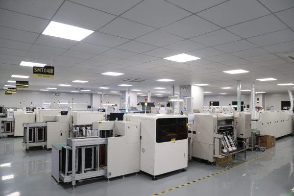
Manufacturing electronics is hard. You worry about defects and high costs. I see many projects fail because of poor planning. You need a clear path to success.
PCBA (Printed Circuit Board Assembly) is the process of soldering electronic components onto a bare PCB. It involves file preparation, SMT mounting, through-hole insertion[^1], and rigorous testing. Mastering this ensures high quality and optimized costs for your electronics manufacturing.
I will show you how to manage this process. You need to understand every step clearly to avoid mistakes. Let's look at the details now.
What exactly is PCBA and how does the core process work?
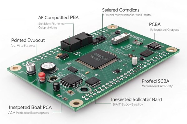
You see a green board with chips. But do you know how it gets there? Misunderstanding this leads to expensive mistakes. You must know the basics first.
PCBA stands for Printed Circuit Board Assembly. It is the finished board after all components are soldered and inspected. It transforms a bare PCB into a functional electronic device using processes like SMT and reflow soldering[^2].
Many people think PCBA is just putting parts on a board. I believe this is wrong. It is a closed-loop system. It connects your files, the factory process, the cost, and the quality control. You cannot view these as separate things. If you change one, the others change too.
I often see clients focus only on the manufacturing speed. They forget that the process starts with data. If your design files are bad, the final product is bad. It does not matter how good my machines are. This is why I say that PCBA is a system engineering task.
We need to look at the difference between PCB and PCBA. A PCB is just the bare board. It has no function. It is like a skeleton. The PCBA is the body with muscles and a brain. It works.
Core Differences and Workflow
| Feature | PCB (Printed Circuit Board) | PCBA (PCB Assembly) |
|---|---|---|
| State | Bare board, no components | Finished board, fully populated |
| Function | Provides electrical pathways | Performs electronic functions |
| Process | Etching, drilling, plating | Solder printing, mounting, reflow |
| Outcome | Passive structure | Active device |
You must understand this flow. It moves from data to bare board, then to component sourcing, and finally to assembly. It is a chain. If one link breaks, the whole chain fails.
What are the 8 critical steps in the PCBA process?
You want consistent quality. But skipping steps causes failures. You need to know the machine workflow to prevent defects. I will explain the standard procedure.
The process includes Solder Paste Printing[^3], SPI, Pick and Place, Reflow Soldering, AOI, Through-Hole Insertion, Wave Soldering[^4], and Functional Testing. Each step requires specific equipment and strict parameter control to ensure connection reliability.
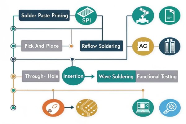
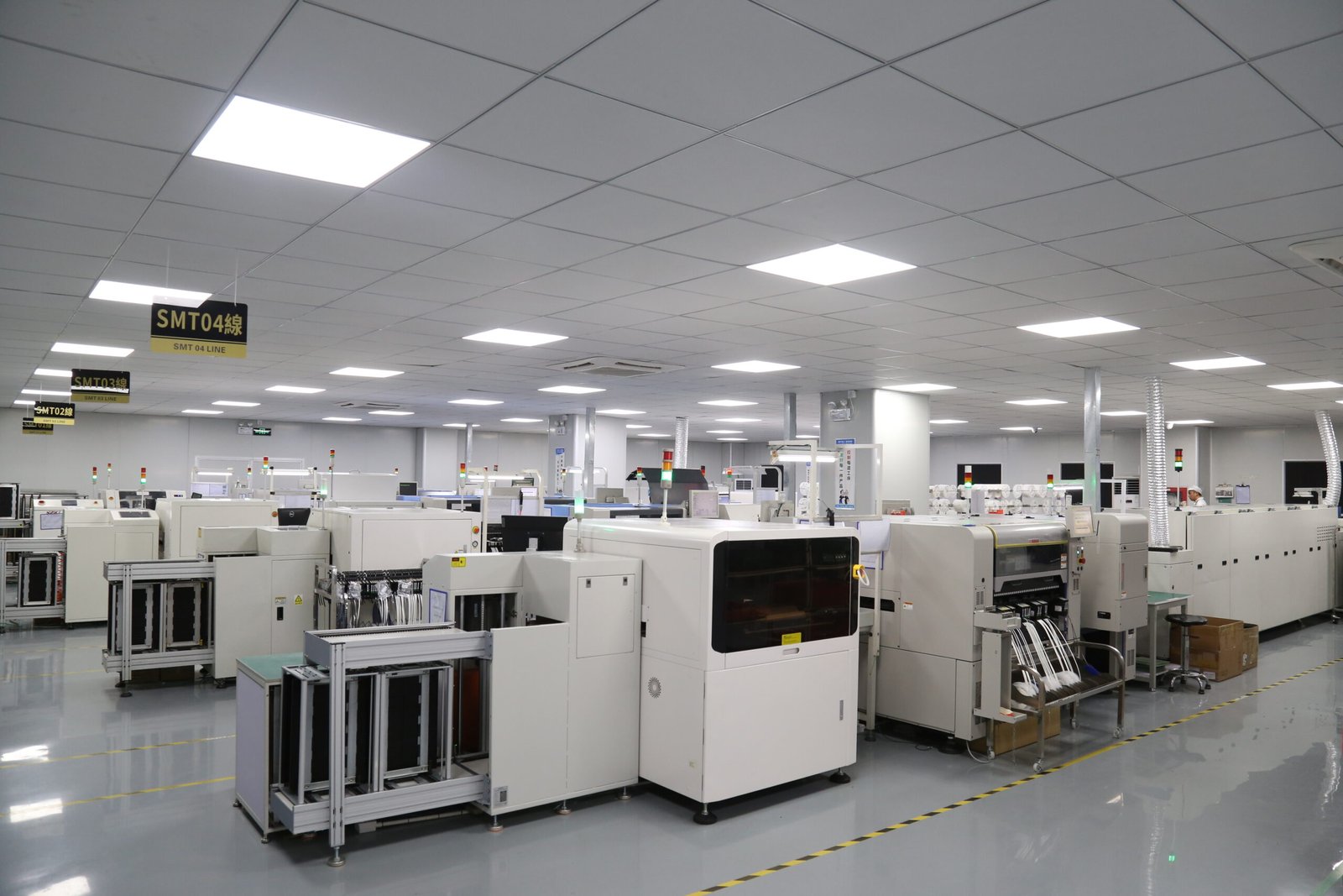
I have walked through my factory floor thousands of times. I see how each machine affects the next one. You need to understand that this is a precise sequence. We cannot change the order.
Step-by-Step Breakdown
- Solder Paste Printing[^3]: This is the most critical step. We use a stencil to put paste on the pads. If the paste is too thick, you get bridges. If it is too thin, the joint breaks.
- SPI (Solder Paste Inspection): We check the paste volume here. A machine looks at every pad. This catches 70% of defects before we even add parts.
- Pick and Place: The robot arm grabs components. It places them on the wet paste. Speed is important here, but accuracy is more important.
- Reflow Soldering: The board goes into an oven. Hot air melts the paste. The temperature profile must be perfect. If it heats too fast, parts crack.
- AOI (Automated Optical Inspection)[^5]: A camera checks the soldering. It looks for missing parts or bad joints.
- Through-Hole Insertion (DIP): Some parts are too big for SMT. Humans or machines insert legs into holes.
- Wave Soldering[^4]: A wave of molten tin solders the legs. This is for the through-hole parts.
- Functional Testing (FCT): We turn the board on. We check if it actually works.
Key Equipment Parameters
| Step | Key Equipment | Critical Parameter |
|---|---|---|
| Printing | GKG Printer | Squeegee pressure & speed |
| Mounting | Yamaha/Juki Mounter | X-Y axis precision |
| Reflow | 10-Zone Oven | Temperature ramp-up rate |
| Inspection | 3D AOI | Camera resolution & lighting |
You must ensure your manufacturer controls these parameters. Ask them about their oven profiles. Ask them about their SPI limits. This shows them you know what you are talking about.
Which files are required for a successful PCBA order?
Missing files delay production. You lose time and money. I often receive incomplete data that stops the whole factory. You must prepare the right package.
You must provide Gerber files for the bare board, a BOM (Bill of Materials) for components, and CPL (Component Placement List) for machine coordinates. Accurate files are the source of cost control and quality assurance.
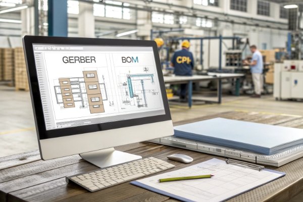
I always tell my clients: "Garbage in, garbage out." The quality of your files determines the quality of your product. This is where cost control really starts. It does not start with negotiating the price. It starts with your BOM.
The Three Pillars of PCBA Data
1. Gerber Files: These are the blueprints. They tell us where the copper goes. They tell us where the holes are. You must include all layers. Do not forget the solder mask layer. Without it, the solder goes everywhere.
2. BOM (Bill of Materials): This is the shopping list. It lists every part. You must be specific. Do not just say "10k resistor." Say "10k, 1%, 0402 package, Yageo brand." If you are vague, we have to guess. Guessing leads to mistakes. A precise BOM prevents us from buying the wrong expensive parts.
3. CPL (Component Placement List): This is the map for the robots. It has X and Y coordinates. It tells the pick and place machine exactly where to drop the chip. It also tells the rotation. If the rotation is wrong, your chip is upside down.
Common File Errors to Avoid
| File Type | Common Error | Consequence |
|---|---|---|
| Gerber | Missing paste layer | Cannot make stencil |
| BOM | No MPN (Part Number) | Wrong part purchased |
| CPL | Wrong origin point | Parts placed off-pad |
I suggest you double-check these before sending them. It saves days of email back-and-forth. It stops production delays.
How do you choose between SMT, Through-Hole, or Hybrid Assembly?
Choosing the wrong method hurts efficiency. Your board might be too big or too weak. You must match the process to the product. I will help you decide.
SMT (Surface Mount Technology) is for small, high-density parts and automation. Through-Hole is for strong mechanical bonds and high power. Hybrid assembly[^6] combines both to balance size, durability, and performance needs.
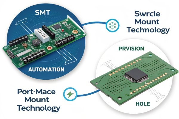
You need to select the process based on your product scenario. Do not just chase efficiency. SMT is fast, but is it strong enough? Through-hole is strong, but is it too slow?
Critical Thinking on Process Selection
I see many engineers try to make everything SMT. They want it to look modern. But sometimes, SMT fails. If you have a heavy connector, SMT solder joints might crack when you plug a cable in. The mechanical stress is too high. In this case, you need Through-Hole technology. The legs go through the board. It is much stronger.
However, Through-Hole takes more space. You cannot put parts on both sides easily. It also costs more because it often needs manual labor. SMT is cheaper for high volume because machines do it all.
Comparison Table
| Feature | SMT (Surface Mount) | THT (Through-Hole) | Hybrid |
|---|---|---|---|
| Component Size | Very small (0201, 01005) | Large, bulky | Mix of both |
| Strength | Moderate | High mechanical strength | Optimized |
| Cost | Low (High automation) | High (Manual labor) | Medium |
| Application | Smartphones, IoT, AI | Power supplies, Connectors | Industrial, Automotive |
Most of my clients use Hybrid. They use SMT for the brain chips and resistors. They use Through-Hole for the power jacks and USB ports. This gives the best balance. You get the speed of SMT and the strength of THT.
How can you ensure quality and troubleshoot common PCBA defects?
Defects destroy your brand reputation. You cannot afford returns. I use strict inspection methods to stop bad boards from leaving the factory. You need to know these tools.
We use AOI (Automated Optical Inspection) for surface checks, X-Ray for BGA chips, and ICT (In-Circuit Testing) for electrical function. Common defects like bridging or tombstoning are identified and fixed early in the process.
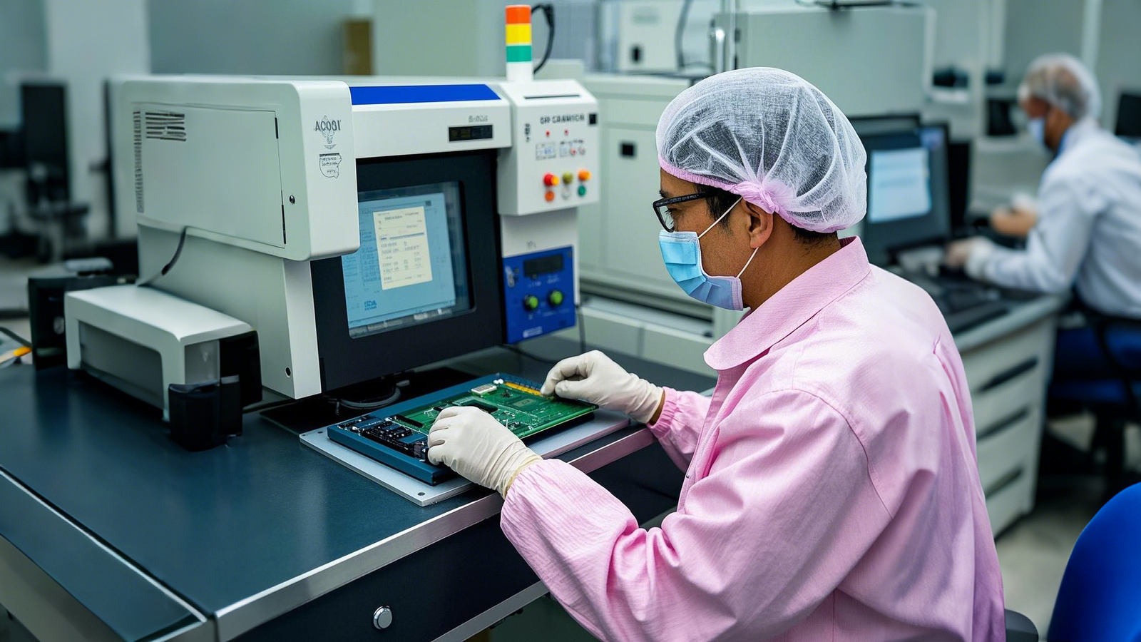
Quality control is not something you do only at the end. It must be a loop. We check, we find a problem, we fix the process. If we find a defect, we don't just fix the board. We ask "why did this happen?"
Inspection Methods Deep Dive
1. Visual Inspection: This is basic. A human looks at the board. It is good for obvious damage. But humans get tired. We miss things.
2. AOI (Automated Optical Inspection): This is the standard. Cameras compare the board to a perfect image. It catches "Tombstoning." This is when a small part stands up on one end like a tombstone. It happens if one pad heats up faster than the other. AOI sees this instantly.
3. X-Ray Inspection: You cannot see under a BGA (Ball Grid Array) chip. The connections are underneath. We use X-Rays to look through the chip. We check for bubbles in the solder. If there are bubbles (voids), the chip will overheat and fail.
Troubleshooting Common Defects
| Defect | Appearance | Root Cause | Solution |
|---|---|---|---|
| Bridging | Solder connects two pins | Too much paste | Adjust stencil aperture |
| Cold Joint | Dull, rough solder | Temp too low | Increase reflow temp |
| Open Joint | No connection | Pad oxidation | Check PCB storage |
I believe that quality control starts with file verification. If we catch a bad footprint in the Gerber file, we prevent thousands of defects.
What are the 6 practical ways to reduce your PCBA costs?
Manufacturing costs eat your profit. You feel the pressure to cut prices. I know how to save money without hurting quality. You need smart strategies.
Optimize costs by standardizing components, panelizing boards[^7] effectively, reducing unique parts in the BOM, avoiding over-specification, ordering in larger batches, and involving your manufacturer early in the design phase.

Cost optimization is tricky. If you cut costs the wrong way, quality drops. You need to optimize the supply chain and the process adaptability.
6 Practical Tips
- Consolidate Your BOM: Do not use ten different types of resistors if you can use five. If you use the same part many times, we buy it in bulk. It is cheaper. It also means fewer feeder changes on the machine. This saves setup time.
- Smart Panelization: Put as many boards as possible on one panel. But be careful. If the panel is too big, it warps in the oven. If it is too small, you waste material. Ask us for the best panel size.
- Use Standard Parts: Custom parts are expensive. They have long lead times. Use standard capacitors and connectors. They are always in stock.
- Avoid Over-Specifying: Do not ask for military-grade PCBs if you are making a toy. Do not ask for gold plating if tin is enough. Pay only for what you need.
- Design for Assembly (DFA)[^8]: Place parts in a way that is easy to assemble. Keep space between parts. If they are too close, we need expensive manual inspection.
- Early Supplier Involvement: Talk to me before you finish the design. I can tell you "Hey, move this chip, it is too close to the edge." This saves you a redesign later.
Impact of Volume
The setup cost is high. We have to program machines and make stencils. If you order 10 boards, the setup cost is high per board. If you order 1000, it is cheap. Plan your volume carefully.
How do different industries apply PCBA solutions effectively?
Every industry has different rules. You cannot use a toy standard for a medical device. I treat every sector with specific care. You need to know your industry requirements.
Consumer electronics focus on size and speed. Industrial boards need durability and heat resistance. Medical devices demand extreme reliability and traceability. We adapt the process to meet these specific industry standards.
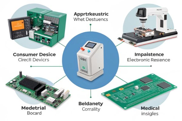
We serve many industries. Each one forces us to think differently. A board for an air conditioner is different from a board for an AI server.
Industry-Specific Requirements
1. Artificial Intelligence & IoT: Here, size is everything. We use HDI (High Density Interconnect) boards[^9]. The components are tiny. We use 0201 or even 01005 parts. The challenge is signal integrity. High-speed signals need perfect impedance control.
2. Automotive & New Energy: Safety is the priority. The board must survive vibration and heat. We use heavy copper PCBs to handle high current. We use strict IPC Class 3 standards[^10]. If a car board fails, people can get hurt.
3. Industrial & Telecommunication: These boards run 24/7. They cannot stop. We focus on thermal management. We might use metal core PCBs[^11] to dissipate heat. The solder joints must be very strong to last for years.
Comparison of Focus Areas
| Industry | Key Priority | Typical Tech | Quality Standard |
|---|---|---|---|
| Consumer | Cost & Size | HDI, Rigid-Flex | IPC Class 2 |
| Automotive | Reliability | Heavy Copper | IPC Class 3 |
| Medical | Safety | Flex PCB | ISO 13485 |
I always ask my client: "Where will this board live?" If it lives in a hot factory, we build it tough. If it lives in a pocket, we build it small.
How do you choose the right PCBA factory for your business?
Choosing a bad partner is a nightmare. Delays and bad quality happen. I suggest looking for specific traits in a manufacturer. You need a reliable partner.
Look for a factory with one-stop capabilities, verified certifications (ISO), transparent communication, and a focus on B2B customization. Avoid retailers. Ensure they handle sourcing, fabrication, and assembly under one roof.
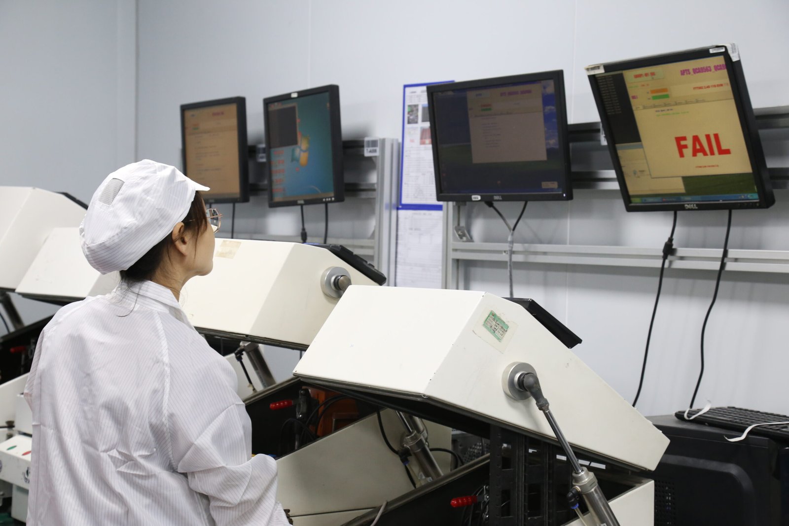
You need a partner, not just a vendor. In the B2B world, stability is key. You don't want a factory that changes prices every week.
Key Selection Criteria
1. One-Stop Solution: Can they do everything? It is better to have one company handle the PCB, the parts, and the assembly. If you split it, you have to manage three companies. If something goes wrong, they blame each other. A one-stop shop takes full responsibility.
2. Factory vs. Broker: Make sure they are a real factory. Ask for a video call. Ask to see the SMT lines. Many "manufacturers" are just trading companies. They add a margin and lose control of quality. We are a factory. We control every step.
3. Supply Chain Strength: Can they get chips when there is a shortage? A good factory has strong relationships with distributors like Digi-Key and Mouser. We can find parts when others cannot.
The Checklist for Vetting
- Certifications: Do they have ISO9001?
- Equipment: Are their machines modern?
- Response Time: Do they reply quickly to emails?
- NDA: Are they willing to sign a Non-Disclosure Agreement to protect your IP?
I believe transparency is the most important thing. If there is a delay, I tell my client immediately. I do not hide it. This builds trust.
What are the most frequently asked questions about PCBA?
You still have doubts. That is normal. I have gathered the most common questions to help you finalize your decision. You need clear answers.
We answer questions about lead times, minimum order quantities, and testing protocols. We also provide checklists for file preparation and defect troubleshooting to help you prepare your order correctly.
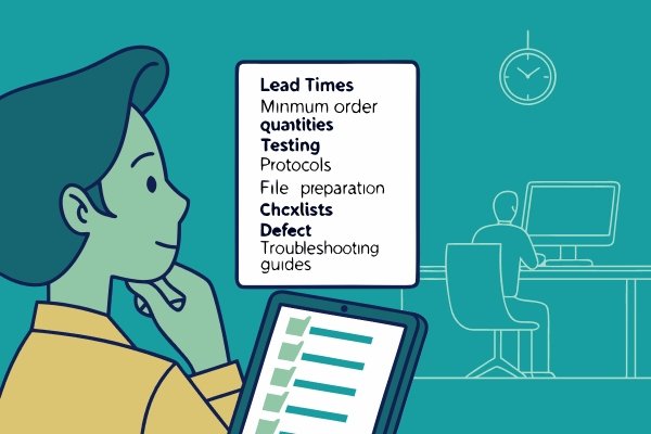
Here are the questions I hear every day.
Common Q&A
Q: What is the typical lead time? A: For prototypes, it is usually 3-5 days. For mass production, it takes 2-3 weeks, depending on component availability.
Q: Do you have a Minimum Order Quantity (MOQ)? A: We focus on B2B. We prefer orders that are not retail. However, we support prototypes for business clients to test their design before mass production.
Q: Can you handle BGA assembly? A: Yes, we have X-Ray inspection to ensure BGA quality. We can handle fine-pitch components.
Q: Do you source the parts? A: Yes, we provide full turnkey services. We source from authorized distributors to ensure genuine parts.
Free Resources for You
To help you get started, I recommend you create a simple checklist before sending files.
- BOM Check: Are all part numbers correct?
- Gerber Check: Are all layers included?
- Quantity: Is the volume clear?
By following these simple steps, you avoid 90% of the common problems.
Conclusion
PCBA is a closed loop of files, process, cost, and quality. Success comes from accurate data and choosing the right partner to manage the entire system efficiently.
[^1]: Through-hole insertion is vital for components that require strong mechanical bonds, ensuring durability in electronic devices. [^2]: Reflow soldering is a critical step in PCBA, ensuring that components are securely attached to the PCB. [^3]: Solder paste printing is the first and most critical step in PCBA, affecting the quality of solder joints. [^4]: Wave soldering is used for through-hole components, providing strong and reliable solder joints. [^5]: AOI is essential for detecting defects in PCBA, ensuring high-quality and reliable electronic products. [^6]: Hybrid assembly combines SMT and through-hole techniques, optimizing for both size and strength in PCBs. [^7]: Panelizing boards efficiently uses materials and reduces production costs, crucial for cost-effective manufacturing. [^8]: DFA optimizes PCB design for easier assembly, reducing costs and improving production efficiency. [^9]: HDI boards allow for high-density component placement, essential for compact and advanced electronic devices. [^10]: IPC Class 3 standards ensure high reliability and performance in PCBs, especially for critical applications. [^11]: Metal core PCBs are used for effective heat dissipation, crucial for high-power and high-temperature applications.

